
Photonics Has a Layout Problem
The hardest step in photonic computing isn't the math or the energy. It's deciding where everything goes.
1. The moment, and what photonic computing actually is
The bottleneck in modern compute is not the math. It is the movement of data.
On a modern AI accelerator, the energy cost of moving an operand from memory to the arithmetic unit can be a hundred to a thousand times higher than the cost of the arithmetic itself, and that ratio has been getting worse with each process node. The math keeps getting cheaper. The hauling does not. Much of the AI infrastructure stack is now being redesigned around this one uncomfortable fact, and the redesign is not subtle.
One response is to stop using electrons for the hauling. A photon traveling through a waveguide doesn't dissipate energy to resistance, doesn't pay a capacitance tax that grows with distance, and (in linear media) doesn't interact with other photons sharing the same physical channel at different wavelengths. A chip whose interconnect, and increasingly whose computation, ran on light would have a meaningfully different energy profile. Not incrementally different. Structurally different.
For about thirty years that argument has been made. Photonic computing has reliably been five years away, a distinction it shared, for a while, with fusion power and self-driving taxis. That's not the case anymore. In April 2025, a Nature paper reported a photonic AI processor that executed ResNet, BERT, and the Atari deep learning algorithm by DeepMind (Lightmatter, Nature 2025). Around the same time, a Munich-based startup, Akhetonics, reported an integrated photonic implementation of a general-purpose all-optical digital processor: a CPU whose digital logic is built entirely from photonic components (Kissner et al., 2024). What used to be conference-talk speculation is now being fabricated and tested on silicon.
Most introductions to photonic computing take this as a cue to sprint toward energy diagrams and inference benchmarks. We're not going to do that. The bottleneck this piece dissects only makes sense once you understand what the building blocks of a photonic chip actually are and why they behave so differently from their electronic counterparts. A few concepts below aren't second nature to readers from software, so we'll build them from one equation almost everyone has seen, and from the physical intuitions hiding underneath it. The vocabulary also happens to be the same vocabulary that shows up in LiDAR, biosensors, and quantum processors, something we'll use in the next section.
A short electrical primer
Here's the thing about the wire problem: you can't reason about why it's so hard to solve without first understanding why wires cost anything at all. The answer is embarrassingly classical. It comes down to three numbers: heat, switching energy, and delay. Know these three quantities and you know why chip designers lose sleep, why photonics is interesting, and why "just make the wires better" stopped being a satisfying answer around the time you were learning to drive.
All three follow from one equation: \(V = IR\).
Heat. Power is energy per unit time, so it is voltage times current:
$$P = IV = I^2R.$$A wire has nonzero resistance, so the current through it dissipates power as heat.
Switching energy. A gate's input acts as a capacitor holding charge \(Q = CV\). Charging it from 0 to V moves each increment \(dq\) across the voltage already present:
$$E = \int_0^Q v\,dq = \int_0^V C v\,dv = \frac{1}{2}CV^2.$$Equivalently, the capacitor ends with total charge CV, added at an average voltage of V/2. This means a voltage transition costs energy proportional to \(CV^2\), which is why switching activity dominates digital power.
Delay. The resistor caps the current near \(V/R\) while the capacitor needs charge \(CV\), so the voltage settles in a time
$$\tau = \frac{CV}{V/R} = RC$$(also known as the time constant), independent of the drive voltage. Exactly, \(v(t) = V(1 - e^{-t/RC})\), with \(RC\) the time constant.
A wire's resistance and capacitance both grow with its length, so a longer wire costs more energy per bit and delivers each bit more slowly.
Here is the consequence that has come to shape chip design. As transistors have shrunk, they've gotten cheaper to switch, but the wires connecting them have not improved at the same rate. A long wire's R and C keep climbing relative to the transistors it links. Designers fight this with repeaters (buffers inserted along a long wire to break it into shorter, faster segments), but repeaters cost area and power of their own. A fix that costs energy to save energy is not obviously a fix; it's a remittance to a different landlord. The net effect, across the last two decades, is that a growing share of a processor's energy and delay budget goes not to computing but to shuttling bits between where they're computed and where they're stored or used. This is the wire problem, or the interconnect bottleneck, and it's the physical reason data movement, rather than arithmetic, has become the binding constraint in modern systems. You can't Moore's-Law your way out of a physics problem.
How photonics changes the picture
A photonic interconnect doesn't carry a current. That one fact eliminates most of the \(V = IR\) machinery from the transport: no \(I^2R\) heat, no \(\tfrac{1}{2}CV^2\) paid along the path, no RC delay compounding with length. Gone. A bit is encoded onto a beam of light, and that light propagates through a waveguide as an electromagnetic field at roughly \(c/n_{\mathrm{eff}}\), about 40% of the speed of light in a silicon waveguide. The light still loses some energy to scattering off fabrication imperfections and to material absorption, but in good silicon waveguides this runs around 1-3 \(\mathrm{dB}/\mathrm{cm}\), low enough that crossing a chip is fairly cheap and, crucially, doesn't compound the way RC does.
A guided optical mode propagates with wavenumber
$$\beta = \frac{2\pi}{\lambda_0} n_{\mathrm{eff}},$$where \(\lambda_0\) is the free-space wavelength. Loss accumulates with distance but at a low per-unit rate; because there's no charge in transit, the dominant electrical penalties (\(I^2R\) dissipation and the length-dependent \(\tfrac{1}{2}CV^2\) and \(RC\) terms) are largely absent from the transport.
The energy cost in a photonic link doesn't disappear; it moves. Instead of being spread along the path, it concentrates at the two endpoints. At the source, a continuous-wave laser supplies the light and a modulator encodes data onto it by changing the refractive index of a short waveguide section under an applied voltage. That modulator has electrodes, and electrodes have capacitance, so the \(\tfrac{1}{2}CV^2\) term doesn't vanish, but it's paid once, at the point of modulation, rather than continuously along the path. State-of-the-art silicon and silicon-compatible modulators have reached the few- to tens-of-femtojoules per bit regime, with research devices pushing lower. At the far end, a photodetector converts the light back into a photocurrent for the electronics to read.
There is no free lunch
It would be easy to stop there and declare photonics the winner. It's also wrong. Photonics doesn't eliminate the cost of moving data so much as trade one set of costs for another, and any honest introduction has to say that plainly.
The laser is the clearest example. The light has to come from somewhere, and the lasers used in these systems are typically only 10-30% wall-plug efficient; most of the electrical power going in is lost before any light reaches the chip. The endpoint conversions cost too: driving a modulator and amplifying a detector's weak photocurrent both require electronic circuits with their own power draw, which is part of why most "photonic" systems today are really electronic-photonic hybrids rather than purely optical. Don't let the press releases oversell you. The components are also large; photonic devices are measured in hundreds of micrometers where transistors are measured in nanometers, and they don't shrink as the process improves. And some components, ring resonators especially, are sensitive to temperature and to small fabrication variations, often needing active tuning to stay on their operating point, which costs more power and, as we'll see in Section 4, makes automated layout genuinely hard.
The honest framing is a trade rather than a miracle. Photonics removes the length-dependent penalties that dominate electrical interconnects and replaces them with fixed overheads at the endpoints, plus a handful of device-level sensitivities you have to manage. Whether the trade pays off depends on the regime. For short, local connections where an electrical wire is already cheap, it often doesn't. For the long, high-bandwidth connections where the wire problem hurts most: chip-to-chip, package-to-package, and increasingly across large dies, it increasingly does, and the balance has been tilting further toward photonics as bandwidth demands rise.
The advantage that tips the balance
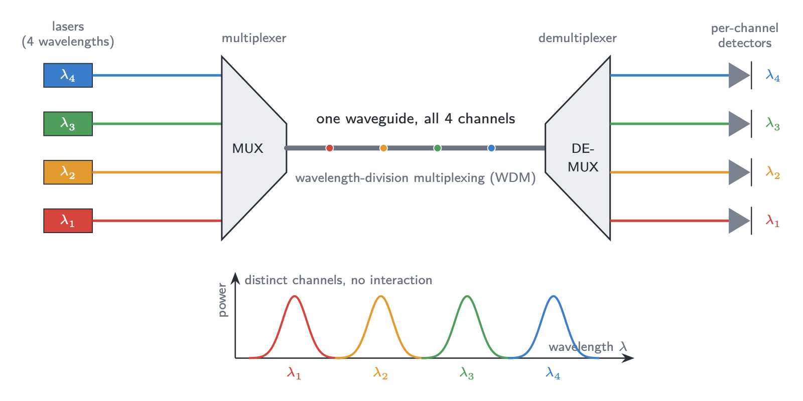
What makes the trade look decisively favorable, not merely competitive, is one property with no close electrical analog. In a linear medium, light at different wavelengths doesn't interact. A single waveguide can carry many independent channels at once: different wavelengths, each modulated and read out independently, all sharing the same glass without knowing the others are there. The channels are mutually invisible. Bandwidth grows by adding wavelengths, not physical wires. This is wavelength-division multiplexing (WDM), the technique behind the long-haul optical networks that already carry most of the internet's traffic, the same physics, scaled down to a chip.
An electrical bus eventually runs out of pins and routing space. An optical waveguide has a great deal of spectral room before it runs short of usable wavelengths. For a workload whose binding constraint is moving large volumes of data, AI inference being the obvious example, that is a kind of structural headroom that process scaling alone cannot provide. Scaling makes transistors smaller. It does not make physics more lenient.
The components
Before the rest of this piece makes sense, you need to know the vocabulary. There isn't much of it. A photonic integrated circuit is assembled from a small number of device types; the same vocabulary shows up in AI accelerators, LiDAR, quantum processors, and biosensors. Same components, wildly different end markets. We'll return to that in the next section, because it changes the economic argument substantially.
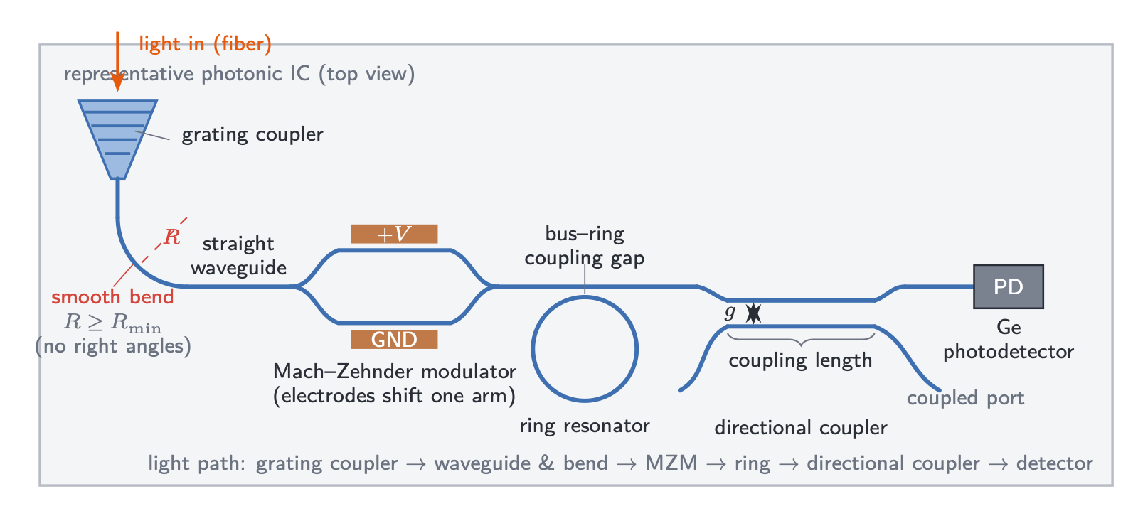
Waveguides are the wires: straight runs, bends, tapers, and specialty structures. Modulators impose information onto the signal, the way transistors gate it in electronics; the two dominant silicon-photonic architectures are the Mach-Zehnder modulator (MZM), which splits light into two arms, perturbs the index in one or both, and recombines them through interference, and the ring resonator modulator, which shifts a small ring's resonance with a tiny index change (Bogaerts et al., 2012). Detectors are germanium-on-silicon photodiodes at the readout. Couplers (grating, edge, and directional) handle the interfaces between fibers, chips, and waveguides. Four device families. That's most of a PIC.
The voltage-induced phase difference between the two arms is \(\Delta\phi\). \(\Delta n_{\mathrm{eff}}\) for silicon plasma dispersion is small, often around \(10^{-4}\) depending on drive and geometry, so \(L\) runs to hundreds of micrometers or more, set by physics rather than lithography, which is why these devices don't shrink with the process node.
Here \(m\) is an integer mode order. Small rings (\(R \sim 5~\mu\mathrm{m}\) in many silicon designs, larger in other platforms) are compact but quite sensitive to temperature, fabrication variation, and stress, a recurring theme.
Put it together. Photonics doesn't make data movement free, but it changes the cost structure in a way that suits the direction computing is heading: pulls the dominant penalties off the interconnect, concentrates what remains at the endpoints, and offers a way to scale bandwidth through wavelengths rather than wires. The math behind these components, the MZM's \(\cos^2\) transfer function and the ring's resonance condition, is not incidental decoration. It is, as we'll see in Section 4, precisely what makes a photonic layout so much harder to automate than an electronic one. Geometry is physics, and physics doesn't get abstracted away just because a tool vendor wishes it would.
What this story leaves out, what almost no introduction to photonic computing bothers to address, is how these chips are actually designed in the first place.
2. The same chip, a dozen industries
It's tempting to treat that design question as a niche concern for AI hardware. It isn't.
The energy argument is what put photonics in the headlines, but the move from discrete optical parts to integrated photonic chips was already well underway before the AI datacenter crowd showed up. FMCW LiDAR uses PICs to steer beams without moving parts; autonomous vehicles are a volume play that has nothing to do with matrix multiply. Lab-on-chip biosensors and gas sensors use them to detect trace molecules in blood or air at sensitivities that would require a small room's worth of bench optics otherwise. Integrated spectrometers are collapsing instruments that used to cost tens of thousands of dollars into something that fits in a surgical suite. Photonic quantum processors are a different animal entirely. Here, the waveguides aren't moving data, they're routing entanglement. And underneath all of it, optical networking has been carrying the world's data traffic for decades; the photonic chip is just the latest layer of that infrastructure closing in on itself. These are not adjacent applications. They are industries with separate customers, separate regulatory regimes, separate funding pools, and in some cases separate physics priorities.
What unites them is not a market thesis; the overall trajectory is clearly up, but the decade's precise numbers are a projection, not a fact, and the spread across analyst estimates is wide enough to park a datacenter in. What unites them is something more structural: a LiDAR beam-steerer, a quantum processor, an on-chip spectrometer, and an AI tensor core are all built from the same small vocabulary of components. Waveguides. Modulators. Resonators. Couplers. Detectors. The same foundry processes. The same design rules. The same physical constraints that make the layout so difficult to automate (and this is, I should note, a bit of foreshadowing here) make it difficult for every single one of them. The bottleneck is not vertical, particular to one industry. It runs horizontally across the whole field. Same chip architecture, same hard step, twelve different markets stuck at it simultaneously.
3. The question nobody asks
In electronics, how a chip gets designed has a boring answer, and the boredom is the point. A designer describes what they want in a hardware description language, and a chain of software, synthesis, placement, routing, timing closure, turns that description into a manufacturable layout with little human intervention at the level of individual wires. The tools, sold by Cadence, Synopsys, and Siemens, are a multi-billion-dollar industry built on decades of refinement. They work well enough that a designer can place a billion transistors without thinking about any of them individually. This place-and-route problem, where each component physically sits and how the wires connect, is, for electronics, solved: not trending toward solution, not improving year over year, but off the list of hard problems entirely. Electronics made it boring on purpose. Decades of unglamorous tool-building, and then one day nobody thought about it anymore. That is the goal. That is the win.
Photonics never got there.
A photonic integrated circuit is still laid out with far more human judgment than a digital electronic chip. Picture what that actually means: a designer opens the layout canvas and starts placing components. One by one. By eye or by script, they position each element, then draw or nudge the waveguides connecting them, deciding at every bend and every crossing whether to tighten the arc or give it more room. Each choice feeds into the next. They check their decisions against the design rules and the loss budget. Run an optical simulation. Find where the design bleeds light it can't afford to lose. Go back. Adjust. Re-route. Run it again. A modest PIC takes days to weeks of this; a complex one, months. And much of that time isn't architecture or simulation. It's layout. It's the crossing-by-crossing, bend-by-bend, rule-check-by-rule-check grind that Cadence automated for electronics thirty years ago. Much of the expertise of these people goes into a task that, in electronics, a script handles before lunch.
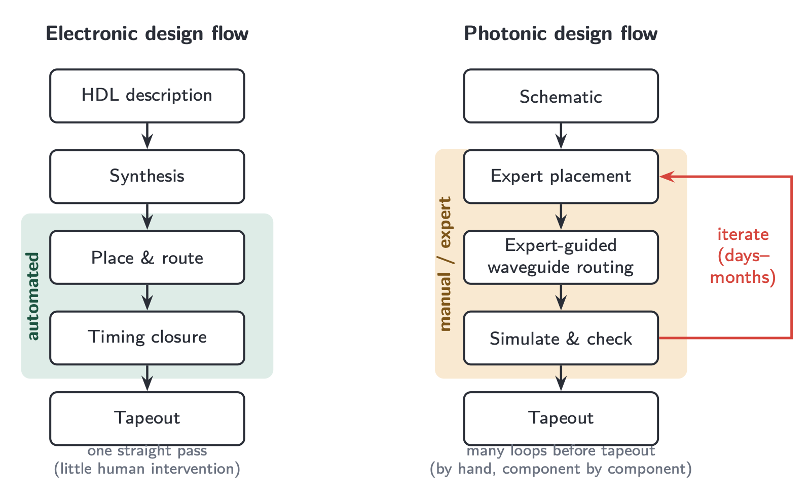
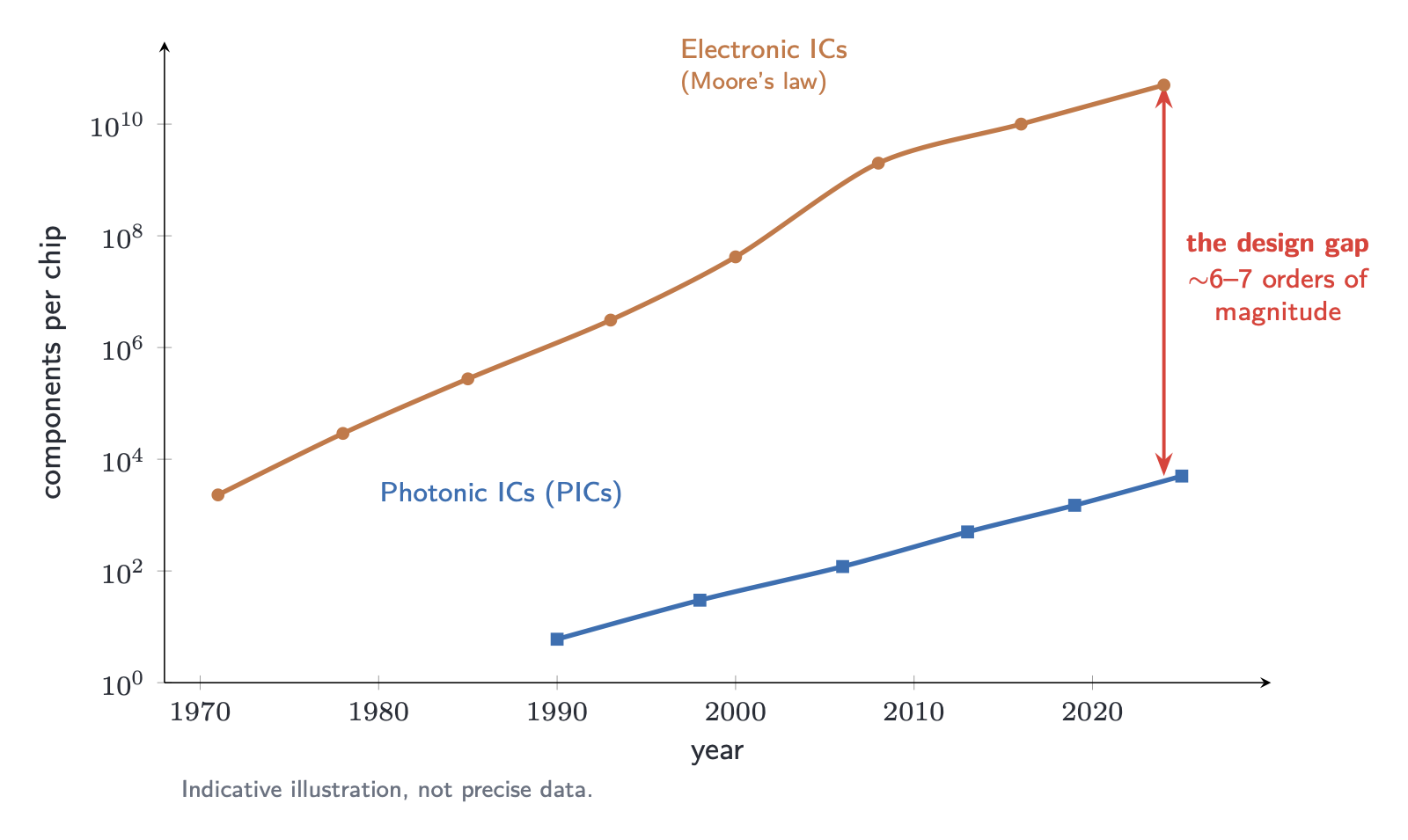
The result is a stark gap in achievable complexity. A leading-edge electronic chip integrates on the order of \(10^{10}\) transistors; a state-of-the-art PIC still typically sits in the hundreds-to-thousands-of-components regime, with the largest academic layout benchmarks now pushing into several-thousand-component designs (Apollo, 2025). Some of that is the size difference between a transistor and a ring resonator. But much of it is simpler than that. Much blunter.
You cannot hand-place ten billion of anything.
Here is why that sentence deserves a moment. Let \(\tau\) be the time to place and route one component by hand and \(N\) the component count, so hand layout costs on the order of \(T \approx N\tau\). Taking \(\tau \approx 5\) minutes of human judgment per component:
- At \(N = 10^3\): \(T \approx 80\) hours, two working weeks. About what a PIC that size can take today.
- At \(N = 10^6\): \(T \approx 40\) years of full-time work.
- At \(N = 10^{10}\): the figure stops carrying meaning.
Workable at a thousand components. Hopeless an order or two above. And electronic chips cleared a billion transistors fifteen years ago.
The natural assumption from electronics is that this is temporary, that photonic EDA is just younger, and the same automation will arrive in time. That is half right. Photonic EDA is younger. But it hasn't simply copied the electronic playbook because the playbook rests on a set of abstractions that the physics of light breaks. To see why, look at what actually happens when light travels through a layout.
4. Where the physics changes everything
Recall that the effective wavelength of telecom light inside a silicon waveguide is hundreds of nanometers (about 650 nanometers for \(n_{\mathrm{eff}} \approx 2.4\), and closer to 450 nanometers in more tightly confined modes) while the waveguide that carries it is about 500 nanometers wide. In electronics the analogous comparison is wildly different: for ordinary chip interconnects, the wire is an abstract conductor whose shape matters through resistance, capacitance, inductance, timing, and crosstalk, not through the detailed wave nature of the signal itself. In photonics, the wave and the structure guiding it are nearly the same size. The geometry is not a container for the signal; the geometry is part of the signal's physics. Everything that follows in this section is a corollary of that one sentence.
Bends
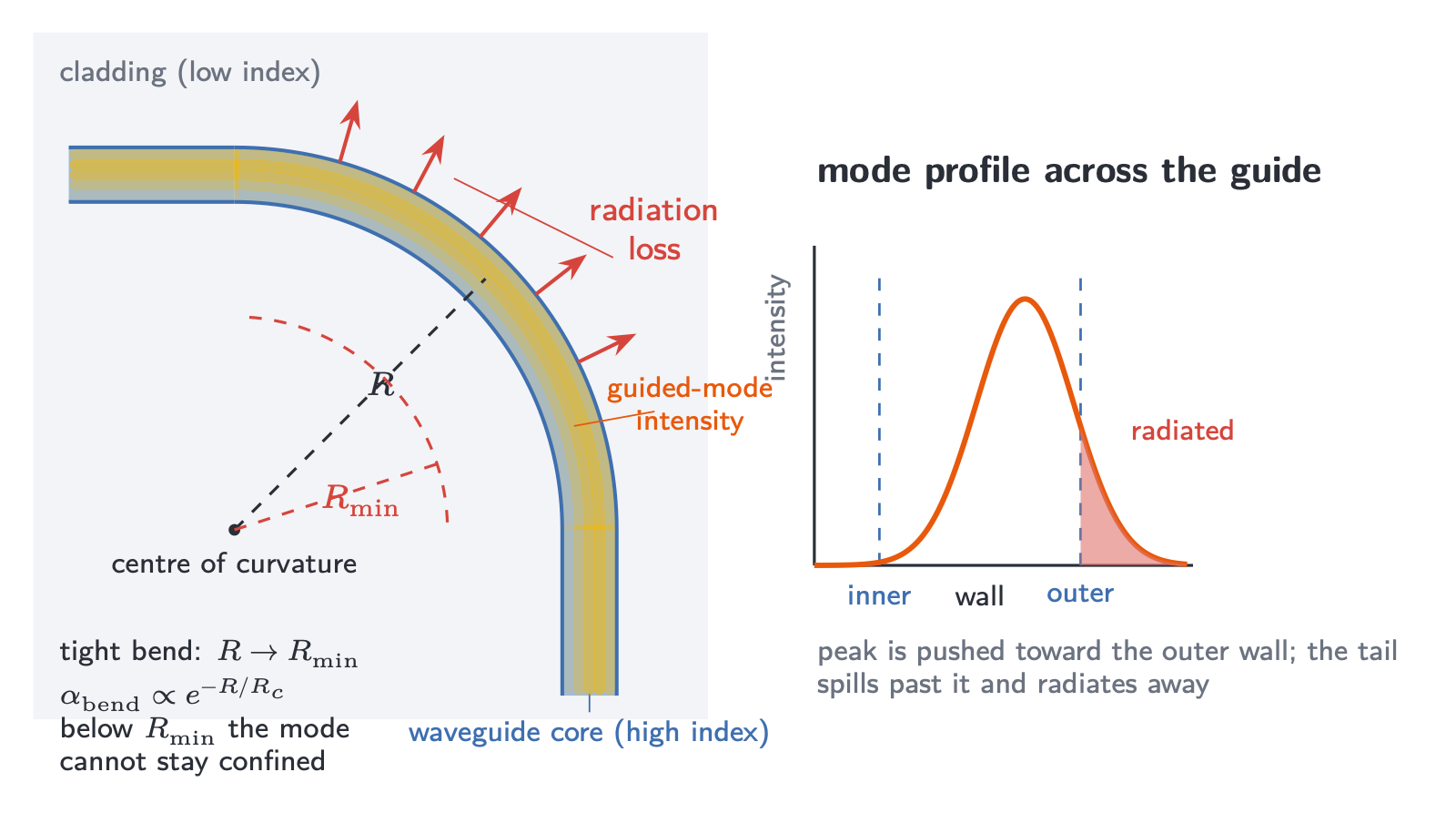
A guided mode is held in the waveguide by the index contrast between core (high refractive index) and cladding (low refractive index), but it is not perfectly confined; its field extends a little into the cladding. When the waveguide bends, the outer edge of the mode has to travel farther to keep pace with the phase front; past a certain tightness it simply cannot, and power radiates away into the cladding. Radiation loss climbs steeply as the bend radius shrinks. The tighter the turn, the more you hemorrhage signal.
Radiation loss rises approximately exponentially as radius decreases:
$$\alpha_{\mathrm{bend}} \propto e^{-R/R_c},$$where \(R_c\) is a characteristic radius set by the index contrast and wavelength. The practical consequence is a minimum usable bend radius, roughly a few micrometers for high-contrast silicon waveguides, and tens of micrometers or more for lower-contrast silicon-nitride waveguides.
There are no right angles in photonic layout. Every turn is a smooth arc with a radius bounded from below by physics, and the lower-loss platforms demand the largest turns. A single bend can consume more chip area than an entire logic gate. Think about what that implies for a layout of hundreds of them.
Adjacency
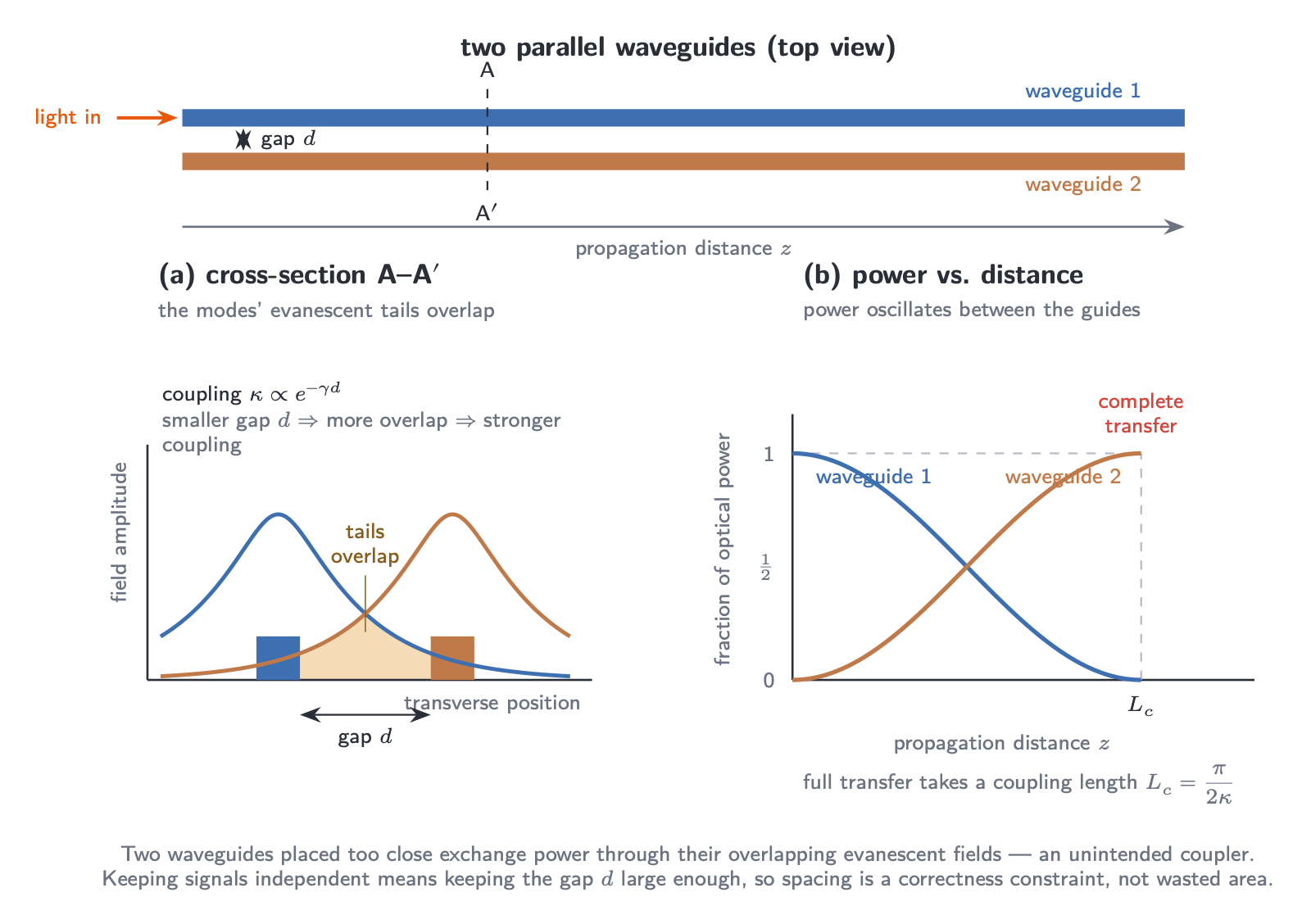
Because the mode's field extends into the cladding, two sufficiently close parallel waveguides do not just sit there minding their own business. Their evanescent fields overlap, and when the two guides are phase-matched, power transfers between them, quietly, continuously, whether you wanted it to or not. This is not crosstalk in the electrical sense; it is an unintended optical coupler. You built a device and didn't mean to.
The coupling strength falls off exponentially with the gap \(d\) between waveguides:
$$\kappa \propto e^{-\gamma d}, \qquad L_c = \frac{\pi}{2\kappa}.$$Complete power transfer occurs over the coupling length \(L_c\). To keep two waveguides effectively independent, their separation must be a few times the mode size, often on the order of micrometers in silicon, depending on geometry and parallel run length, and the longer they run in parallel, the more carefully that gap must be controlled.
In electronics, you can pack parallel wires tightly; the penalty is manageable capacitive coupling, timing noise, and power, all of which circuit design has evolved to handle. In photonics, every pair of nearby waveguides is an unintended optical device. There is no "managing" it. The layout has to be spaced to prevent it from happening in the first place, which means white space is not waste: it is correctness.
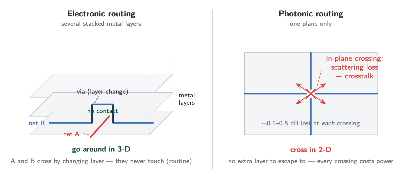
Crossings
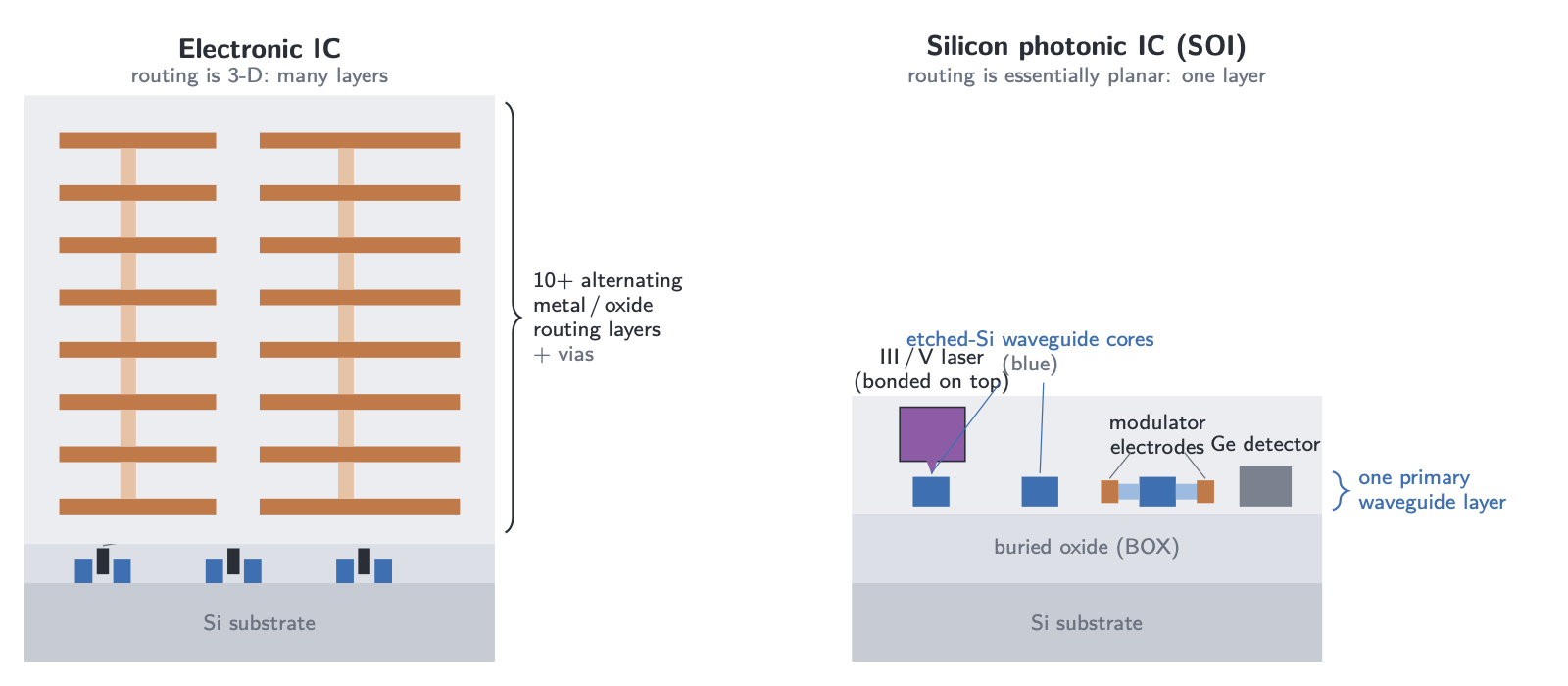
This is the deepest difference, and it follows from fabrication as much as physics. An electronic chip has a dozen or more metal layers stacked vertically and joined by vias, so when two wires must cross, one simply changes layer. Crossing is not completely free, but it is routine; routing is a three-dimensional search through a forest of layers. Photonic chips, by contrast, usually have one primary waveguide layer or only a small number of optical routing layers. Two waveguides that need to cross often must do so in the same plane, and an in-plane crossing is a small scattering event: some light is lost, some couples into the wrong path as crosstalk.
Each crossing contributes insertion loss, often quoted in the 0.1-0.5 dB range for ordinary crossings and lower for carefully optimized crossing structures, plus crosstalk. The losses accumulate along a path:
$$\mathrm{loss}_{\mathrm{path}} \approx N\times(\mathrm{loss\ per\ crossing}).$$A path with 50 crossings at 0.3 dB each loses about 15 dB, meaning roughly 97% of the optical power is gone.
Taking ideas from the electronic cousin, stacking waveguides into multiple optical layers to escape this is possible and actively researched, but it is not the same thing as adding another CMOS metal layer. Optical layers must be separated enough to avoid unwanted evanescent coupling, vertical transitions between layers add loss and process complexity, and dense multilayer optical routing is not a default capability across foundry platforms. So routing in photonics is, to first approximation, a planar problem: connect every component in a single plane while minimizing unavoidable crossings. Minimizing crossings in a planar layout is a genuinely hard combinatorial problem, and it is one a human currently solves by hand, crossing by crossing.
Length is signal
In electronics, a longer wire delivers its bit a little later. Annoying, but the bit arrives intact, a one is still a one. In photonics, the signal can be a wave with a phase, and the phase accumulates along every millimeter of the path. Length is not a latency. Length is a phase shift. And phase shifts change the answer.
The phase accumulated over a waveguide of length \(L\) is
$$\phi = \beta L = \frac{2\pi}{\lambda_0}n_{\mathrm{eff}}L.$$Two paths between the same points whose lengths differ by \(\Delta L\) emerge with a phase difference
$$\Delta\phi = \frac{2\pi}{\lambda_0}n_{\mathrm{eff}}\Delta L.$$Because \(n_{\mathrm{eff}}/\lambda_0\) is large, even a sub-micron length difference produces a meaningful phase shift.
So exactly how small is "meaningful"? A Mach-Zehnder modulator or interferometer swings from full transmission to complete extinction when its two arms differ in phase by \(\pi\), which from Equation 8 is a path-length difference of
$$\Delta L = \frac{\lambda_0}{2n_{\mathrm{eff}}} = \frac{1550~\mathrm{nm}}{2 \times 2.4} \approx 323~\mathrm{nm}.$$A third of a micron, less than one wavelength of light in vacuum, shorter than the width of the waveguide itself, is the difference between on and off. Let that land. A great many photonic devices, Mach-Zehnder interferometers, arrayed-waveguide gratings, almost anything built on interference, encode information in exactly these path-length differences. For those circuits, "route a waveguide from A to B" is not a complete instruction. It never was. The length of the route is a designed quantity, as much as any transistor parameter, and two paths that look topologically equivalent to a router are not optically equivalent at all. Routing cannot be decoupled from circuit function the way it is in electronics, where the router is free to take any legal path that meets timing. In photonics, there is no such freedom. The route is part of the design.
Components don't shrink
Finally, and this one is almost insulting given everything else, the components themselves are large and stubbornly fixed in size. As Equation 3 showed, a silicon Mach-Zehnder modulator is hundreds of micrometers to millimeters long because the underlying index change is small. A ring resonator's circumference is set by its resonance condition. A grating coupler needs roughly ten micrometers of periodic structure to match a fiber mode. None of these shrink with the process node. Decades of silicon scaling made transistors smaller; the wavelength of light didn't care. A photonic layout is therefore a sparse arrangement of large, irregularly shaped, fixed-footprint blocks, connected by curved, non-crossing, length-constrained waveguides, a placement-and-routing problem with almost none of the regularities that let electronic EDA scale to a billion transistors.
Put these together and the conclusion is hard to avoid. Every abstraction that makes electronic place-and-route automatable, wires as shapeless conductors, free crossings between layers, routes interchangeable as long as they connect the right points, components that shrink and tile with the process node, fails in photonics. Not softens. Not gets harder. Fails. And each failure traces back to the same physical root: the wavelength of light is comparable to the structures carrying it, so geometry and physics cannot be separated. Bends cost area and loss. Adjacency builds unwanted devices. Crossings are lossy events that accumulate. Path length is a circuit parameter. Components are fixed in size by physics, not process. Photonic layout is not electronic layout made smaller, or younger, or less mature. It is a different problem, one that the abstractions of electronics were never built for, and that is precisely why it has resisted the automation that transformed everything else.
5. What's available today
If photonic layout is a different problem from electronic layout, the question is what tools exist for it and how far they get. The field has made more progress than it's usually credited with, but that progress still stops well short of what the industry needs.
The commercial tools
The major EDA vendors all sell photonic design environments: Synopsys (OptoCompiler over OptoDesigner), Cadence (a Virtuoso-based electronic-photonic flow), Siemens (L-Edit Photonics and LightSuite), alongside specialist tools like Luceda's IPKISS and the open-source gdsfactory, now a de facto standard in academic and startup work. These are not purely manual drawing tools. Synopsys, Cadence, and Siemens all automate major parts of PIC design, including routing, layout generation, simulation, implementation, and verification. Much of the drawing and checking is already automated.
But that is not the same as digital place-and-route. In complex PICs, the hard part is not just drawing legal waveguides; it is choosing the global placement and routing topology so thousands of paths fit under bend-radius, spacing, crossing-loss, crosstalk, phase, thermal, and foundry constraints. The researchers building the next generation of PIC routing tools are not shy about why: available PIC layout tools remain mostly schematic-driven and have not relieved the burden of manual waveguide planning and layout (Zhou et al., 2025).
This distinction matters. The gap is not "there are no photonic layout tools." That would be false. The gap is that there is no broad photonic equivalent of digital place-and-route: no general engine that takes a large photonic netlist, understands the physics, proposes a global placement, chooses a routing topology, budgets loss and phase, and hands off a fabrication-ready layout across arbitrary PIC domains. The productivity gain from today's tools is real; the gap from "tool that assists a human laying out a chip" to "tool that lays out the chip" is not closed in any commercial product.
The academic frontier
The most serious attack on that gap comes from academia, and one group has built most of a vertical stack in about two years: the ScopeX lab at Arizona State. The headline is that they have actually automated placement and routing for large PICs: GPU-accelerated, routing-informed global placement (Apollo, 2025) followed by curvy-aware detailed routing that emits design-rule-clean GDS for real-world photonic circuits (LiDAR, 2025). That alone is a meaningful bar to clear. The rest of the stack, simulation surrogates, heater and driver metal routing, fabrication-aware inverse design, extends the coverage further, and the whole thing is openly published, largely open-source, plugged into gdsfactory. It is real, fabrication-aware progress toward automated layout, and should be treated as such.
It also belongs to a single methodological school. The engine, in every case, is physics-driven analytical optimization: gradient descent for placement, A* for routing, adjoint methods for devices, with neural networks used as accelerators or surrogates, not as the thing that generates the layout.
Three important things are absent from the stack: generative models, pretraining that transfers across designs, and learning that amortizes experience from one chip to the next. The benchmarks lean on photonic AI cores and interconnects rather than the full LiDAR, sensing, and quantum range that shares the same physics. And it is research-grade, open-source prototypes, not productized tools with the foundry-PDK coverage, verification, and support tapeout demands. The distance from a router that clears academic benchmarks to a tool a company stakes a fabrication run on is wide, and historically it is companies, not papers, that close it.
So the state of the art is two-sided. Commercial tools are productized but assistive; they automate the drawing, checking, and implementation, not the global deciding. Academic tools are beginning to automate the deciding, impressively, but are narrow in scope and far from production. Neither does for a thousand-component PIC across arbitrary domains what electronic EDA does routinely for a billion-transistor chip.
6. The lesson from electronics
Electronics faced the same structural problem and solved it with a method the field spent years being suspicious of. Worth examining.
Macro placement, where large functional blocks sit on a die, is a hard combinatorial problem that, like photonic layout, long resisted full automation and survived on human expertise. In 2021 a Google team published a method in Nature that reframed it as reinforcement learning: an agent places blocks one at a time, gets rewarded on the quality of the finished layout, and, critically, gets better as it sees more designs, carrying what it learned from one chip to the next rather than starting each engagement from scratch (Mirhoseini et al., 2021). The field's initial reaction was skeptical, then grudging, then unavoidable. Later named AlphaChip, it produced layouts that didn't look like a human's and, on some metrics, beat them.
Then it shipped. AlphaChip layouts have been taped out across multiple TPU generations and in Axion datacenter CPUs. MediaTek extended it to accelerate development of its advanced chips. The conversation moved from "is this real?" to "how do we use it?" Learning-based layout is not a research curiosity parked in a Nature paper. It is running in production silicon right now.
Two lessons carry to photonics, and one warning.
Lesson one: a hard, expertise-bound layout problem turned out to be a tractable target for a learning-based method, not because RL is magic, but because placement quality is scoreable. What you can score, you can optimize. What you can optimize repeatedly, you can learn. Photonic layout is the same class of problem: loss, crossing count, footprint, phase error, thermal sensitivity, and routability are all numbers. You can define a reward. The door is open.
Lesson two: the value came from transfer, and that is exactly the property the analytical tools from academia don't have and can't easily acquire. An A* router is just as ignorant at the thousandth PIC as it was at the first; it accumulates no institutional memory, carries no intuition across designs, and improves only when a human hand-tweaks its heuristics. A learning-based method compounds. Every layout it sees is leverage on the next one. That asymmetry is the whole game.
The warning: none of this transfers for free, and anyone telling you otherwise is selling something. The lesson is not "do AlphaChip for photonics." Macro placement in electronics has a comparatively clean objective function, a mature simulation stack, and decades of training data in the form of known-good layouts. Photonics has none of those things handed to you. The lesson is narrower and more demanding: learning-based, experience-compounding methods are a credible, and almost entirely untried, way to attack this class of problem, and making them work means solving the photonic-specific difficulties head-on rather than just porting an electronic recipe and hoping the physics cooperates.
7. What we're betting on
Put the last two sections together. The analytical tools work but don't transfer. The electronics precedent says transfer is where the leverage is. No public system has yet made modern generative layout synthesis the central engine for broad, physics-constrained photonic layout. That is the opening, and we are taking it.
Why not simply "reinforcement learning for PICs"
The obvious move, given the precedent, is to copy it: reinforcement learning, an agent placing components for a reward. We think that's the wrong default. Not wrong everywhere. Wrong here, for a reason specific to this problem.
RL earns its keep on sequences of discrete decisions with rewards that are hard to differentiate through, where you literally cannot compute a gradient toward improvement and must learn by stumbling trial and expensive error. Much of photonic layout isn't like that. Component positions are continuous. The loss from a bend or a coupling gap is a smooth function of geometry. The governing physics is, to a good approximation, differentiable. On a differentiable objective, gradient methods are faster and more sample-efficient than RL, which is exactly why the analytical tools from academia work as well as they do. Reaching for RL as the primary engine is not bold; it is throwing away the gradient information the physics hands you for free, then paying trial-and-error tuition for knowledge you already owned.
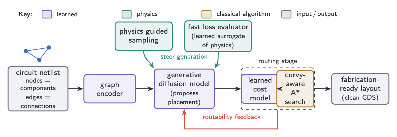
So the question isn't "RL or not." It is how to combine a model that learns across many designs with the differentiable physics that makes the problem tractable. That is what we mean by physics-informed generative design, and each half constrains the other.
Generative, because the leverage is in transfer
The property we want is the one analytical tools lack and the electronics precedent rewards: amortizing experience across designs, so the system produces a good layout for a new circuit quickly rather than re-solving from scratch. Every time an A* router finishes a PIC, it forgets everything. We want a system that does the opposite.
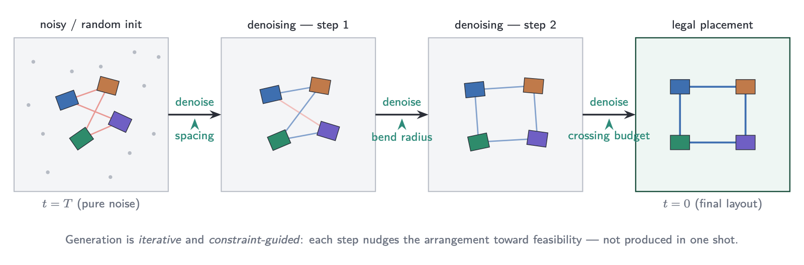
That points to generative models, trained on many circuit/layout pairs, learning the distribution of good layouts, proposing one for a new circuit in a forward pass or a few. The most promising direction, in our view, is diffusion models, for a concrete reason: a diffusion model generates by iterative refinement, and that loop is a natural place to inject constraints. The precedent exists in electronics: researchers at UC Berkeley were able to train a diffusion model to place new circuits zero-shot, using guided sampling in place of RL, on synthetic data and transferring to real circuits. That recipe hasn't been brought to photonics at the same level, where the constraints differ but the structure of the approach carries over. The synthetic-data angle is worth flagging here and returning to later: it is one credible answer to photonics' missing layout corpus.
The arrangement space is what makes a learned prior necessary rather than merely convenient. Consider just the ordering problem, ignore geometry entirely, just line up N components. The count of orderings grows as N!. A hundred components gives \(100! \approx 10^{158}\) distinct orderings. There are perhaps \(10^{80}\) atoms in the observable universe. You will not search that space blindly. You will not search it cleverly. You will not search it at all; you need a strong prior on where good layouts live, and you build that prior by training across many designs. The math is not here to impress; it is here to kill the idea that a sufficiently fast search engine solves this.
Physics-informed, because the constraints are not optional
A model trained naively on layouts would learn to imitate their appearance, not respect the physics. In photonics, that distinction is fatal: a layout that looks right but violates a bend radius or underestimates a coupling length is not a slightly suboptimal layout. It is a broken chip. The physics cannot be a post-processing check. It has to enter the model's reasoning directly, in three places.
In the sampling: minimum bend radius, spacing, crossing budget, and length-matching act as guidance gradients that nudge each refinement step toward feasibility. The model proposes; the physics steers. In the loss: training penalizes predicted optical loss, crossing count, phase error, and footprint, quantities computed from geometry, not merely deviation from example layouts. The model is rewarded for layouts that are physically good, not just statistically typical. And in the simulator: evaluating a candidate requires fast optical feedback, which is where neural-operator surrogates and differentiable compact models earn their place, fast stand-ins for expensive electromagnetic or circuit-level simulation, sitting inside the training and generation loops where full simulation would be ruinously slow.
Where RL and classical methods still fit
This is not a rejection of RL or of the analytical tools. It is an allocation: each method to the part it suits, not the part it can technically be tortured into.
Routing topology is genuinely combinatorial and non-differentiable, a legitimate home for RL or learned-cost search built on the existing curvy-aware routers. Detailed geometric refinement, once the topology is fixed, is differentiable and well served by exactly the gradient-based optimization the analytical school has spent years perfecting. The generative model's job is the part neither handles: producing, from experience across many designs, a strong global arrangement to start from, so the downstream stages refine rather than search blindly. Each tool does what it is actually good at.
The bet, stated plainly: the right architecture is a hybrid, generative where transfer matters, differentiable where the physics is smooth, discrete-search where the problem is genuinely combinatorial, unified by physics that informs every stage. Not elegant for its own sake. Correct for the problem.
Why this is the right bet for a horizontal problem
One more reason to prefer a generative approach, and it is the one that turns a useful engineering bet into a structural one.
The bottleneck is horizontal. The same physics, bend radius, coupling, crossing loss, phase, mode confinement, constrains layout across AI cores, LiDAR arrays, biosensors, and quantum chips. An analytical tool tuned to one application's benchmark has to be substantially re-engineered for the next. That is not a theoretical complaint; it is the reason the academic tools, as impressive as they are, remain narrow in scope. You do not solve a horizontal problem with a vertical tool.
A model that learns the underlying distribution of good photonic layouts, across component libraries, foundry platforms, and application domains, generalizes the way the problem demands. The same property that makes it good at transferring across designs makes it good at transferring across the whole industry. These are not two separate arguments. They are the same argument at two different scales.
That is the thesis. Not a better router for one kind of chip. A learned, physics-informed generator for photonic layout as a general problem, the kind of system the breadth of this field has always needed and has never had.
8. Summary
The throughline is this: photonic layout is hard because light does not let geometry be abstracted away. A waveguide is not just a wire. Its bend radius determines loss. Its spacing determines coupling. Its crossings scatter power. Its length sets phase. Its components are large because their dimensions answer to wavelength, resonance, interference, and mode confinement, not to lithography, not to a router's convenience, not to any abstraction a designer might prefer. The layout is not a container for the circuit; it is part of the circuit's behavior. Every geometry decision is also an optical decision. There is no separating the two.
That is why the missing layer in photonic design is not faster drawing software. Faster drawing is not the problem. The hard decision is physical: where should the components sit so the routes are short but not sharply bent, close but not coupled, connected but not full of lossy crossings, compact but still phase-correct? Those constraints conflict. They have to be balanced simultaneously, before detailed routing, before verification, and often before a human designer has any intuition about which floorplan is worth spending days refining. Today's tools help implement a design once that judgment has been made. The unresolved problem is the judgment itself.
This is also why copying electronic place-and-route is not the answer. Electronics gives us the proof of concept: layout automation can unlock an order-of-magnitude jump in design complexity. But photonics changes the terms of the problem completely. The useful abstraction is not "wires connecting blocks." It is a physical field propagating through geometry. Any serious automation layer has to know that from the start, that a cleaner-looking route may be optically worse, that a millimeter of length mismatch can shift a phase and break the circuit, that two paths laid down too close become an unintended coupler, and that one crossing avoided is sometimes worth more than an entire footprint improvement. These are not edge cases. They are the ordinary texture of photonic layout.
That is the case for a physics-informed generative layout system. Not a heuristic with a better objective function. Not a reinforcement learning agent trained on one chip family. A generative model, because the search space of viable photonic placements is vast enough that no designer and no classical search can explore it from scratch at scale, and because a system trained across many designs learns where good layouts tend to live, and can transfer that knowledge to the next design instead of starting over. Physics-informed, because in photonics a plausible-looking layout is worthless if it violates the wave behavior that makes the circuit work. This is not a domain where you can run the optimizer first and check the physics later. The physics has to be in the loop from the first refinement step to the last. And the model should not try to replace simulation, foundry rules, or existing EDA infrastructure, because the layer we are trying to occupy is the one that doesn't exist yet.
The bet is not that machine learning makes physics go away. It is the opposite. The bet is that the only way photonic layout scales is by putting the physics closer to the center, woven into every proposal the generator makes from the first refinement step, not bolted on as an afterthought once placement is already done. If photonics is going to move from the hundreds or thousands of components today's best chips contain to the complexity its applications actually demand, the field needs tools that treat geometry as physics, not as drawing. That is not a software problem. It is not a compute problem. It is a problem of what you build the automation around. This piece has been circling that bottleneck from the first section. It is the one worth attacking directly.
If any of this resonates, whether you design PICs and feel the layout grind firsthand, work on the methods that could change it, or simply want to understand why photonic design is as hard as it is, we'd like to hear from you. The problems here don't have obvious answers, and the people who care about them are scattered across disciplines. Good conversations are how things move, let's talk!